As promised in my previous post this post will go in-depth on the internals of the T1600 PSU.
Most of my work was done using the FIVPS2 revision of the board but most of it applies to the FIVPS3 and FIVPS4 revisions as well. There are only minor changes, a couple of the dual capacitors (the 12V and 5V rail) have been replaced by a single, larger capacitor and the SMD 5V regulator for the SUB-battery was replaced by a TO-220 package.
There are some other minor differences but the principle and circuit diagram should apply, just bear in mind the component values might be different.
Before we start
I will give a brief description of what the circuitry is and how it works, followed by an excerpt from the schematic. The full schematic and preliminary troubleshooting guide can be found on GitHub.
I have tried to label all the signals as best I could, some may be however be missing.
The troubleshooting guide is still an early version, there will be changes made.
Having said that, any corrections or suggestions are very much welcomed, please open an issue on GitHub.
Let’s dive in
Let’s start at the beginning. The T1600 has a single 12V, 2A powersupply brick that connects to the PSU PCB through a barreljack connector. There is some common mode filtering, a current sense resistor and a resistor devider to sense the input voltage. Nothing really special.
From there we follow the “VSUPP_L” net (named as such because it is the “low side” of the current sense resistor) to the SUB battery and main battery charge/discharge circuitry.
Main batteries and supply block
The main charge/discharge circuit connects directly to the main batteries through a pair of current limiting resistors and a pair of 22Ohm current-sense resistors. The MOSFETs control the charge rate (fast-charge or trickle-charge) by bypassing the current limiting resistors on demand. From there a diode network is used to isolate the batteries and the main supply and connects to the main 10A fuse.
VSUPP_L also connects to the fuse through a diode.
After the fuse there is a smoothing capacitor and from there the main powersupply runs to the rest of the circuit (V+(MAIN)).
Something to be aware of is that V+(MAIN) can be either 12V from the DC-IN barreljack or whatever the battery voltage is at that time (ususally around 7V).
SUB battery block
The SUB battery is charged directly from the VSUPP_L net through current limiting resistors, it is not fused with respect to the DC-IN barreljack.
It is also charged from V+(MAIN), this provides a trickle-charge when the computer is not plugged in and turned off.
When the computer is running (either from battery or from mains) the SUB battery is charged from the +12V output rail.
The voltage is then regulated down through a linear regulator to provide the backup RAM voltage RAMV (5V). This voltage is always present when either the SUB battery or main batteries are charged or the computer is plugged in to mains.
The charge controller
From the DC-IN section V+(MAIN) connects to various components, including the main charge controller IC.
This IC is a 4-bit microprocessor (not to be confused with a microcontroller) which is running on 5V provided by a linear regulator. It is running at a 500KHz clockrate.
This IC is always on when the main batteries are charged or the machine is plugged in to mains. It controls the power-up of the switchmode controller IC, regulates the charge/discharge of the main batteries and drives the indicator LEDs.
This IC is also responsible for the power-off and low battery beeps through the PC speaker.
It comunicates with the switchmode controller through some kind of 8-bit parallel interface
The current sense network
As this is a “Intelligent power supply” the charge controller monitors the main input current and battery charge/discharge currents.
The main current is fed into a op-amp configured as a differential amplifier, it is using high-side sensing.
The battery current is also fed into a op-amp differential amplifier but this is referenced to ground so it is using low-side sensing.
The output of these op-amp and resistor networks is fed to the charge controller’s analog inputs.
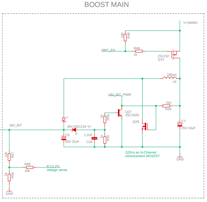
The main boost converter
V+(MAIN) is fed into the main boost converter.
As stated previously, V+(MAIN) can be either 12V from the AC adapter or whatever the battery voltage is. This boost converter steps that up to 18V to provide a stable and well-known voltage to the other switching converters.
This boost converter is turned on on powering up the PSU and is the first converter to start switching. It’s output voltage is sensed by a voltage devider and fed back into the main switchmode controller.
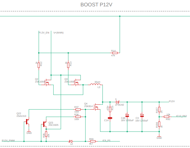
The 12V boost converter
The 12V boost converter is also gated, it is controlled by the switchmode controller. It is the last boost converter to be powered up after all other voltages are withing specification.
All output boost, buck or buck/boost converters are controlled by the main switchmode controller through a push-pull transistor pair.
The 12V output is also sensed through a voltage devider which feeds into the main switchmode controller.
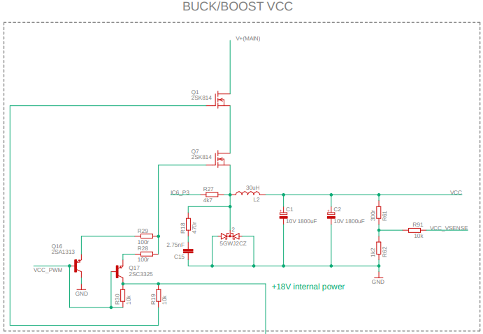
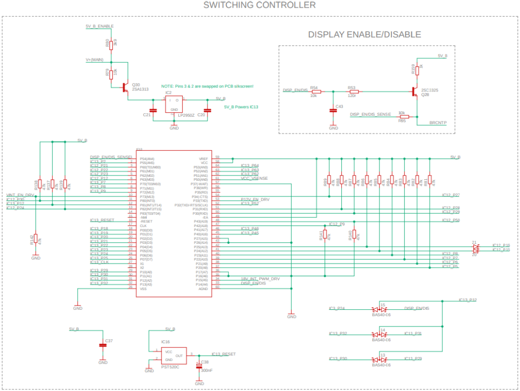
The VCC (5V) buck converter
VCC is generated by another gated converter only this time it is a buck-type.
The MOSFET responsible for enabling this converter is controlled directly by the 18V internal supply.
Like with the 12V converter, this one is controlled through a pair of push-pull transistors and it’s votlage is sensed by a voltage devider who’s output is fed back to the switchmode controller
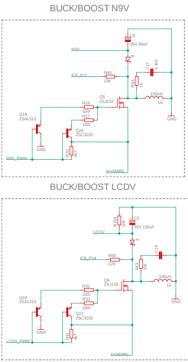
The negative voltage buck/boost converters
The negative rails (-9V and -22V) are generated by two buck/boost converters. The output of the converter is fed back to the switchmode controller through a single resistor and an inverter.
The switchmode controller microprocessor
The main switchmode controller is a 8-bit microprocessor. This IC receives all the analog values from the output of the switching converters and drives the enable signal and PWM for the 18V converter, the enable signal for the 12V converter and the enable signal for the LCD backlight.
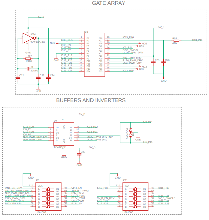
It communicates with a proprietary Toshiba gate array to drive the PWM signals. It’s 20MHz clock signal is also routed through the gate array.
It also communicates with the charge controller IC through a 8-bit parallel interface.
Gate array and buffers/inverters
The gate array IC is what actually drives the PWM signals for the switching converters. The PWM signals for -9V and -22V are inverted before being sent through a MOSFET array that in turn drives the push-pull transistor pairs.
The inverter also receives the output of the -9V and -22V converters and feeds it back into the gate array IC.
The 20MHz clock for the switchmode controller microprocessor is also fed through the gate array.
Output connector
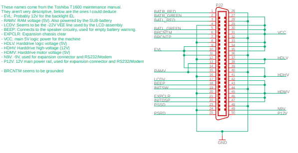
The main connector connects to the system bus flat-flex and provides all the signals and voltages to the rest of the computer. It’s pinout is listed and I have tried to decypher the cryptic names from the Toshiba T1600 Maintenance manual.
A few other bits and bobs
There are some parts of the schematic not covered in this post.
The main reason is I don’t really understand what it is they exactly do.
If anyone can explain this part i’d be happy to do mark it clearly in the schematic and do a follow-up post on it.
Closing thoughts
Though it might seem daunting at first to troubleshoot these boards there really isn’t that much to it.
In the end it is just a collection of switching converters controlled by two microprocessors.
Searching the web for hours on end and hitting the last page of the Google results a couple of times has unfortunately not turned up any information on the proprietary Toshiba gate array. I have not analysed the signals going between it and the switchmode controller IC as it didn’t seem useful in troubleshooting these boards.
Most, if not all, components on these boards are still available or have modern replacements, with the exception of the two microprocessors and the gate array. If any of these three ICs is damaged then that’s it, the board is unfixable. (don’t throw it out yet though!)
Some of the parts, especially some MOSFETs have become hard to find and very expensive. This makes just replacing them as a matter of cause not economically viable and thus thorough troubleshooting and replacing only what is damaged would be advisable.
It is also not impossible to come up with a new design using off-the-shelf components. Ignoring the battery charging circuitry would make that a quite simple design though it would require desoldering the original connector for re-use on the new board as these are pretty much impossible to find in quantities less than 2000.
It is ofcourse possible to create a complete drop-in replacement board, including chare circuitry and logic but that is both beyond my skill level and too time consuming. It would also not be cheap to get built so troubleshooting and repairing would still be the more economic route.
If you have any questions or comments or would like some more information on this or other projects, please feel free to contact me.
I’m currently working on setting up a contact form on this site, that should be available in the next couple of days.